| |
|

|
PRESS RELEASE
|
|
|
|
|
| |
|
|
ASMPT introduces ALSI LASER1206
Fully automatic laser dicing and grooving
Singapore, September 10, 2025 – ASMPT Semiconductor Solutions launches the ALSI LASER1206, its latest system for bare wafer handling and separation under Class 1000 cleanroom conditions, at SEMICON Taiwan 2025. Under the theme “Empower the Intelligence Revolution,” the next-generation laser dicing and grooving platform will be showcased at Booth L0716, Level 4, TaiNEX 1 in Taipei from September 10 to 12. ALSI LASER1206 addresses the growing demand from semiconductor companies specializing in advanced packaging to deliver solutions for growth markets such as AI and smart mobility. This new system, featuring patented multi-beam laser processing technology, with fully automated film frame and bare wafer handling, expands the company's portfolio with a focus on front-end processes.
The next-generation LASER platform has been specifically engineered to meet the increasingly complex requirements of IDM and Foundry semiconductor companies for laser dicing and grooving of wafers. This innovative system delivers precision and performance that is unparalleled in the industry, enabling processing of a wide range of semiconductor materials used in Advanced Memory, Logic, AI and Power applications. The patented UV laser technology achieves maximum precision with minimal heat impact, thereby reducing burr formation and die strength degradation. The device has an integrated wafer coating and cleaning station and offers numerous options for fully automated handling of film frames and bare wafers. The positioning accuracy of the planar motion system is < 1.5 μm. For grooving, wafers from 60 to 800 μm can be processed, while for dicing, the wafer thickness ranges from 20 to 200 μm.
“The new platform is our contribution to the hardware needs of the AI revolution. It combines high-precision laser processing with intelligent automation to support the next generation of semiconductor manufacturing”, says Patrick Huberts, Head of Business and Marketing at ASMPT ALSI. "It is the ideal platform for applications in advanced packaging, AI, and power automotive and mobile applications. And, not to forget, it is the top solution for preparing plasma dicing with maximum yield."
|
|
|
|
About ASMPT Limited (“ASMPT”)
ASMPT Limited is a leading global supplier of hardware and software solutions for the manufacture of semiconductors and electronics. Headquartered in Singapore, ASMPT’s offerings encompass the semiconductor assembly & packaging, and SMT (surface mount technology) industries, ranging from wafer deposition to the various solutions that organize, assemble and package delicate electronic components into a vast range of end-user devices, which include electronics, mobile communications, computing, automotive, industrial and LED (displays). ASMPT partners with customers very closely, with continuous investments in R&D helping to provide cost-effective, industry-shaping solutions that achieve higher productivity, greater reliability, and enhanced quality. ASMPT is a founding member of the Semiconductor Climate Consortium.
To learn more about ASMPT, please visit www.asmpt.com.
About ASMPT Semiconductor Solutions (“ASMPT SEMI”)
ASMPT SEMI is the leading provider of forward-looking solutions for advanced packaging and semiconductor assembly. With its commitment to innovation and customer satisfaction, ASMPT SEMI offers a comprehensive range of products and services that meet the evolving needs of the microelectronics industry. Expert knowledge covers areas such as flip-chip and wafer-level packaging, advanced interconnect technologies, and more. ASMPT SEMI’s state-of-the-art solutions enable customers to achieve higher performance, greater reliability, and improved cost-efficiency in the manufacturing of their semiconductor devices.
ASMPT SEMI sees itself as a pioneer and driving force of the Intelligence Revolution. With its advanced packaging and assembly technologies, the business segement creates the invisible connections that enable intelligent applications in Artificial Intelligence, Smart Mobility, and Hyperconnectivity.
For more information about ASMPT SEMI, visit semi.asmpt.com.
|
|
|
|
|
|
| |
|
|
|
|
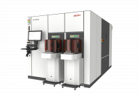
Download:
JPG | RGB | 300dpi | 4,3 MB
ALSI LASER1206, the fully automatic laser dicing and grooving system from ASMPT.
Image source: ASMPT
|
|
| |
|
|
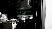
Download:
JPG | RGB | 300dpi | 8,7 MB
The ALSI LASER1206 Pre-Alignment Station detects wafer notches and flats and precisely aligns the wafer for the subsequent laser dicing or grooving process.
Image source: ASMPT
|
|
| |
|
|
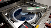
Download:
JPG | RGB | 300dpi | 11,7 MB
The integrated Coating and Cleaning Station of the ALSI LASER1206 enables precise application of protective coatings and reliable removal of particles and residues – ensuring optimal wafer quality and maximum yield.
Image source: ASMPT
|
|
| |
|
|
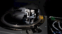
Download:
JPG | RGB | 300dpi | 3,0 MB
The fully automated ALSI LASER1206 system employs patented multi-beam UV laser technology for high-precision wafer dicing and grooving with minimal heat impact – ideally suited for Si, SiC, GaN and other advanced semiconductor materials.
Image source: ASMPT
|
|
| |
|
|
| |
|
|
Unsubscribe from ASMPT media information
If you would like to stop receiving media informations from ASMPT in the future, please send an e-mail to hightech_communications@htcm.de and we will remove your e-mail address from the ASMPT press mailing list.
Unsubscribe from all media informations of our press agency
If you would like to stop receiving media informations from HighTech communications in the future, please send an e-mail to hightech_communications@htcm.de and we will remove your e-mail address from the entire HighTech press mailing lists. |
|
|
|
|
|
|
|
|
|
|
|