| |
|

|
PRESS RELEASE
|
|
|
|
|
| |
|
|
Highly flexible die and flip-chip bonder for co-packaged optics production
AMICRA NANO – Hybrid bonding for data highways
Munich (Germany), November 19, 2024 – The high-precision AMICRA NANO die and flip-chip bonder has been specially developed for the production of co-packaged optics where which optical and electronic components are integrated in a common housing. With its exceptional process stability and a placement accuracy of ±0.2 μm @ 3 σ, this innovative bonding system is ideally equipped for the communication technology of the future.
Co-packaged optics manufacturing is a key process in the production of compact, miniaturized components for today's high-performance data centers and networks that require energy-efficient and high-performance data transmission with minimal latency. To shorten the electrical signal paths, chips and optical interfaces are tightly integrated in a very small space.
“The complexity of semiconductors is constantly increasing and poses enormous challenges, especially with regard to bonding technology,” explains Dr. Johann Weinhändler, Managing Director of ASMPT AMICRA and responsible for ASMPT’s Semiconductor Solutions Division in Europe. “The chips have more and more inputs and outputs, but they must not get any larger. This means that ever finer structures have to be processed with high precision, and this is exactly why we have developed the AMICRA NANO.”
Stable connections with no solder or glue
The NANO die and flip-chip bonder overcomes these challenges by employing an innovative hybrid bonding technology that does not require any solder paste or glue. Instead, it creates stable mechanical and electrical connections with atomic diffusion.
Precision is the prerequisite for further miniaturization
While hybrid bonding enables a high degree of miniaturization, it requires exceptional placement accuracy – in part, because the components no longer center themselves during the heat treatment. The AMICRA NANO places dies from wafers or waffle packs with an accuracy of ±0.2 µm and bonding forces ranging from 0.1 to 20 N, achieving a throughput of 200 to 400 components per hour. With specifications like these, the machine is aimed at the high-mix/low-volume market, for example for chip sets, small lots, prototypes, or feasibility studies for new processes.
The AMICRA NANO achieves its high precision with four high-resolution camera systems that monitor the process from die pickup to final alignment and inspection. Thanks to the machine’s unique design, it is possible to map both the element being placed and the substrate through the bond head at any time. The machine even has an infrared illumination system that penetrates the dies.
Highly flexible technology with an ultra-clean process environment
The machine is also exceptional with regard to its flexibility because it can handle direct and indirect hybrid bonding as well as various soldering and gluing processes. The AMICRA NANO offers three different heating options, including laser soldering and UV curing. Since many processes are highly sensitive to contaminants, the machine is equipped with a HEPA filtering and ionization system that ensures a high-purity operating environment.
Fast computers need fast communication
Hybrid bonding will soon be crucial wherever maximum performance is required in the smallest of spaces – for example, in high-performance and quantum computers, AI systems, IoT devices, or autonomous vehicles. “In particular, converting electrical into optical signals and vice versa is becoming increasingly important, for which light-emitting and light-sensitive components must be placed with exceptional precision,” Dr. Weinhändler sums up. “Having this fast fiber-optic communication technology at your disposal is essential if you want to exploit the potential of future data centers to the fullest.”
|
|
|
|
About ASMPT Limited (“ASMPT”)
ASMPT Limited is a leading global supplier of hardware and software solutions for the manufacture of semiconductors and electronics. Headquartered in Singapore, ASMPT’s offerings encompass the semiconductor assembly & packaging, and SMT (surface mount technology) industries, ranging from wafer deposition to the various solutions that organise, assemble and package delicate electronic components into a vast range of end-user devices, which include electronics, mobile communications, computing, automotive, industrial and LED (displays). ASMPT partners with customers very closely, with continuous investment in R&D helping to provide cost-effective, industry-shaping solutions that achieve higher productivity, greater reliability, and enhanced quality. ASMPT is also a founding member of the Semiconductor Climate Consortium.
ASMPT is listed on the Stock Exchange of Hong Kong (HKEX stock code: 0522), and is one of the constituent stocks of the Hang Seng TECH Index, Hang Seng Composite MidCap Index under the Hang Seng Composite Size Indexes, the Hang Seng Composite Information Technology Industry Index under the Hang Seng Composite Industry Indexes, the Hang Seng Corporate Sustainability Benchmark Index, and the Hang Seng HK 35 Index.
To learn more about ASMPT, please visit us at asmpt.com.
About ASMPT Semiconductor Solutions (“ASMPT SEMI”)
ASMPT SEMI is the leading supplier in advanced packaging and semiconductor assembly solutions. With a commitment to innovation and customer satisfaction, ASMPT SEMI provides a comprehensive range of products and services that cater to the evolving needs of the microelectronics industry. Their expertise spans across areas such as flip-chip and wafer-level packaging, advanced interconnect technologies, and more. ASMPT SEMI's cutting-edge solutions enable customers to achieve higher performance, increased reliability, and improved cost-efficiency when producing their semiconductor devices.
For more information about ASMPT SEMI, visit semi.asmpt.com. |
|
|
|
|
|
| |
|
|
Global ASMPT Press Office:
ASMPT Ltd., Susanne Oswald, Rupert-Mayer-Strasse 48, 81379 Munich, Germany
Phone: +49 89 20800-26439
E-mail: susanne.oswald@asmpt.com, Website: asmpt.com |
|
|
|
|
|
| |
|
|
|
|
Download:
JPG | RGB | 300dpi | 8,9 MB
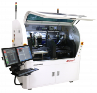
The AMICRA NANO high-precision die and flip-chip bonder was specifically designed for the production of co-packaged optics and features a placement accuracy of ± 0.2 µm @ 3 σ.
Image source: ASMPT
|
|
| |
|
|
| |
|
|
Unsubscribe from ASMPT media information
If you would like to stop receiving media informations from ASMPT in the future, please send an e-mail to hightech_communications@htcm.de and we will remove your e-mail address from the ASMPT press mailing list.
Unsubscribe from all media informations of our press agency
If you would like to stop receiving media informations from HighTech communications in the future, please send an e-mail to hightech_communications@htcm.de and we will remove your e-mail address from the entire HighTech press mailing lists. |
|
|
|
|
|
|
|
|
|
|
|